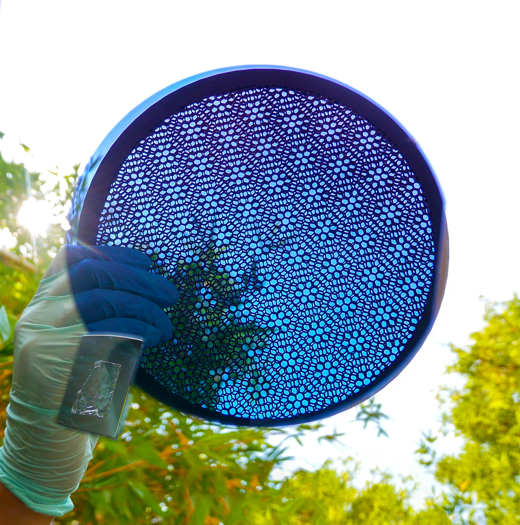
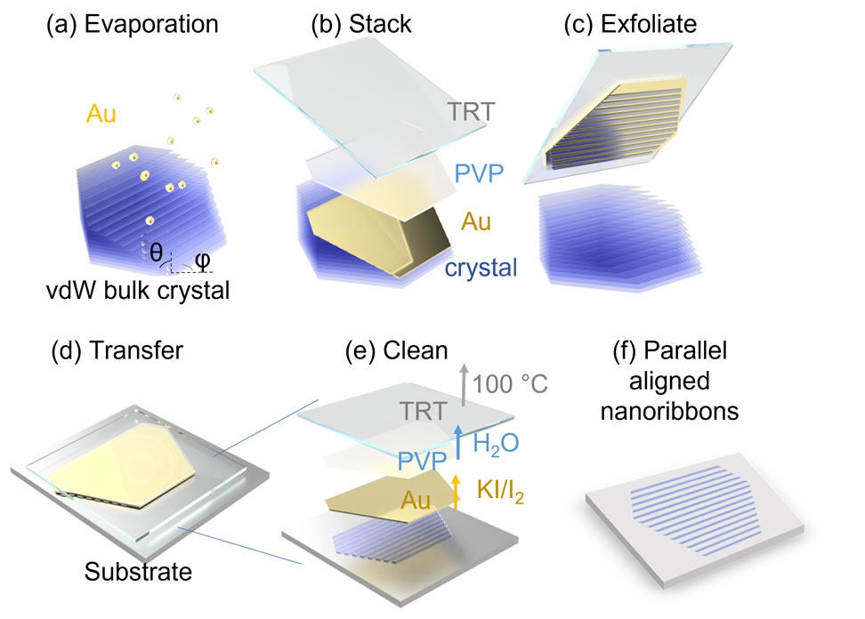
2D monolayers and few-layer flakes with atomic-scale thickness exhibit tunable electronic properties and strong light-matter interactions, making them ideal platforms for realizing high-efficiency transport, ultrafast optical tuning, and novel quantum phases for next-generation information processing and optoelectronic technologies. However, their advancement has been fundamentally constrained by challenges in material availability and quality. We developed metal-assisted exfoliation techniques producing a broad range of high-quality single-crystal 2D flakes with macroscopic-scale dimensions, near-unity yield, and tunable thickness from monolayers to few-layers. 1D Nanoribbons with atomic thickness and nanometer width is another family of low-dimensional confined structure with unique quantum phenomena that surpass their bulk and monolayer counterparts. However, only very few types of nanoribbons are synthesized. We developed a universal exfoliation technique to obtain a wide variety of high-quality single-crystal nanoribbons, from insulators to semiconductors, directly from their bulk van der Waals (vdW) crystals. The flat, aligned nano ribbons with high aspect ratio facilitates study of electronic and optical properties under tunable confinement, strain, and edge configurations for devices.
Moiré superlattices formed by twisted vdW interfaces with nanoscale periodicity offer a promising platform for realizing a wide range of emergent strongly correlated and topological quantum phases. However, again a major bottleneck is sample availability and reproducibility. Conventional fabrication methods, such as exfoliation/tear-and-stack, suffer from extremely low yield (<0.001%), contamination, restricted sample sizes (µm), and instability in twist angle control. To overcome these limitations, we developed a deterministic synthesis method that enables precise and scalable fabrication of a broad range of highly uniform moiré structures, covering transition metal dichalcogenide (TMDC), graphene, and hBN, reaching unprecedented macroscopic dimensions (millimeters to centimeters) with near-unity yield. This breakthrough facilitates comprehensive structural and electronic characterization via electron diffraction, X-ray diffraction, and high-resolution angle-resolved photoemission spectroscopy.
The ongoing and future work will leverage our existing building blocks above and construct artificial superlattices throughout a comprehensive library of 1D/2D/3D low dimensional systems, with diverse nanoscale alignments and symmetries. Such collection will enable systematic exploration of light-matter coupling and designer quantum phases at different levels of precisely engineered nanostructures on a macroscopic, synthetically tunable scale.
Selected Publications
· Saunders, A. P., Chen, V., Wang, J., Li, Q., Johnson, A. C., McKeown-Green, A. S., Zeng, H. J., Mac, T. K., Trinh, M. T., Heinz, T. F., Pop, E., and Liu, F. Direct exfoliation of nanoribbons from bulk van der waals crystals. Small 20(47), 2403504 (2024).
· McKeown-Green, A. S., Zeng, H. J., Saunders, A. P., Li, J., Shi, J., Shen, Y., Pan, F., Hu, J., Dionne, J. A., Heinz, T. F., Wu, S. M., Zheng, F., and Liu, F. Millimeter-scale exfoliation of hbn with tunable flake thickness for scalable encapsulation. ACS Appl. Nano Mater. 7(6), 6574–6582 (2024).
· Liu, F. “Mechanical Exfoliation of Large Area 2D Materials From VdW Crystals”. Prog. Surf. Sci. 100626 (2021).
· Liu, F., Wu, W., Bai, Y., Chae, S., Li, Q., Wang, J., Hone, J., and Zhu, X.-Y. “Disassembling 2D van der Waals Crystals into Macroscopic Monolayers and Reassembling into Artificial Lattices”. Science. 367, 903–906 (2020).